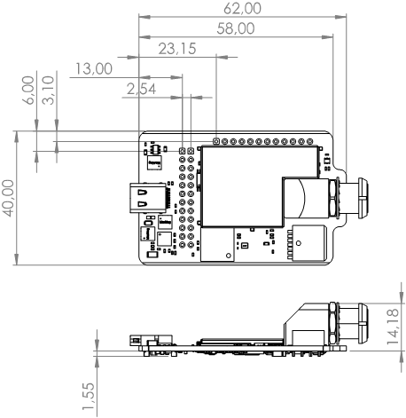
EmStat4M Specifications
This page will detail the technical specifications of the EmStat4M Low Range (LR) and High Range (HR) potentiostat modules. This page is based on the datasheet provided on the EmStat4M product page.
Features
Analog
-
±5 V (LR) or ±8 V (HR) compliance
-
single current measurement channel with max. current of ±30 mA (LR) or ±200 mA (HR)
-
impedance measurements between < 0.1 Ω up to 1 GΩ at frequencies from 0.016 Hz to 200 kHz
-
resolution of 92 fA on lowest current range (LR)
-
16-bit analog-to-digital converter (ADC)
-
1 auxiliary analog input 0 - 3 V
-
1 auxiliary analog output 0 - 3 V (12-bit)
Supported Techniques
The EmStat4M supports the following electrochemical techniques:
Voltammetric Techniques:
-
Linear Sweep Voltammetry (LSV)
-
Cyclic Voltammetry (CV)
-
Fast Cyclic Voltammetry (FCV)
-
AC Voltammetry (ACV)
Pulsed Techniques:
-
Differential Pulse Voltammetry (DPV)
-
Square Wave Voltammetry (SWV)
-
Normal Pulse Voltammetry (NPV)
| These methods can all be used in their stripping modes which are applied for (ultra-) trace analysis. |
Amperometric Techniques:
-
Chronoamperometry (CA)
-
Zero Resistance Amperometry (ZRA)
-
Chronocoulometry (CC)
-
MultiStep Amperometry (MA)
-
Fast Amperometry (FAM)
-
Pulsed Amperometric Detection (PAD)
Galvanostatic Techniques:
-
Linear Sweep Potentiometry (LSP)
-
Chronopotentiometry (CP)
-
MultiStep Potentiometry (MP)
-
Open Circuit Potentiometry (OCP)
Other Techniques:
-
Mixed Mode (MM)
-
Potentiostatic and Galvanostatic Impedance Spectroscopy at fixed frequency or frequency scan vs: (EIS/GEIS)
-
Fixed potential or fixed current
-
Scanning potential or scanning current
-
Time
-
-
Fast EIS/GEIS (FEIS/FGEIS)
-
Very low interval fixed-frequency measurements
-
Pin functions
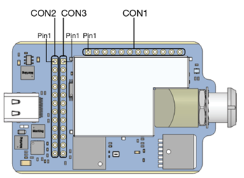
| Pin | Name | function |
|---|---|---|
Con1_1 |
D3 |
Digital GPIO |
Con1_2 |
D2 |
Digital GPIO |
Con1_3 |
D1 |
Digital GPIO |
Con1_4 |
D0 |
Digital GPIO |
Con1_5 |
5V_In |
5V power supply connected internally to USB Vbus |
Con1_6 |
DGND |
PCB common GND plane, digital zone |
Con1_7 |
D4 |
Digital GPIO |
Con1_8 |
SENSE |
Potentiostat Sense Electrode |
Con1_9 |
AGND |
PCB common GND plane, Analog zone |
Con1_10 |
WE |
Potentiostat Working Electrode |
Con1_11 |
RE |
Potentiostat Reference Electrode |
Con1_12 |
CE |
Potentiostat Counter Electrode |
Con2_1 |
TxD |
UART Transmit |
Con2_2 |
RxD |
UART Receive |
Con2_3 |
E_UNIPOLAR_OUT |
E monitor, scaled to a voltage between 0 and 3, centered around 1.5 V where: |
Con2_4 |
I_BIPOLAR_OUT |
Potentiostat measured current (scaled), this pin has a 1 kOhm output impedance |
Con2_5 |
D5 |
Digital GPIO |
Con2_6 |
DGND |
PCB common GND plane, digital zone |
Con2_7 |
nRESET |
Active low reset |
Con2_8 |
nDWNLD |
Active low FW update |
Con2_9 |
ADC_in |
Auxiliary ADC input |
Con2_10 |
DAC_out |
Auxiliary DAC out |
Con2_11 |
DGND |
PCB common GND plane, digital zone |
Con2_12 |
5V_In |
5V power supply connected internally to USB Vbus |
Con3_1 |
CTS |
UART Clear To Send |
Con3_2 |
RTS |
UART Ready to Send |
Con3_3 |
SDA_EXT |
I2C SDA. Internally pulled up to 3.3V via a 10K resistor |
Con3_4 |
SCL_EXT |
I2C SCL. Internally pulled up to 3.3V via a 10K resistor |
Con3_5 |
Reserved |
Reserved |
Con3_6 |
Reserved |
Reserved |
Con3_7 |
E_SET |
External potentiostat voltage setpoint control |
Con3_8 |
n3.3VD_SHDN |
Active low Shutdown. Internally pulled up to 5V with 100K resistor. Pulling to GND disables all power on the ES4 |
Con3_9 |
D6 |
Digital GPIO |
Con3_10 |
3.3V_OUT |
3.3V digital supply. From a switching regulator on the ES4. Draw maximum 50 mA from this pin |
Con3_11 |
VPST- |
Potentiostat negative power rail. Draw maximum 20 mA from this pin. |
Con3_12 |
VPST+ |
Potentiostat positive power rail. Draw maximum 20 mA from this pin. |
Absolute maximum ratings
| Parameter | Rating |
|---|---|
V_IN to GND |
-0.3 V to +5.5 V |
Analog Input Voltage to GND |
-0.3 V to +3.6 V |
Digital Input Voltage to GND |
-0.3 V to +3.6 V |
Total Positive GPIO Pins Current |
50 mA |
Total Negative GPIO Pins Current |
-50 mA |
Storage temperature |
-65 °C to +100 °C |
Operating temperature |
-40 °C to +85 °C |
Hand soldering (single pin) |
400 °C for 10 s |
ESD Human Body Model (HBM) |
4 kV |
ESD Field-Induced Charged Device Model (FICDM) |
1 kV |
Electrical specifications
| Parameter | Min | Typical | Max | Unit | Details |
|---|---|---|---|---|---|
ADC |
|||||
Data Rate |
1M |
SPS |
|||
Resolution |
16 |
Bits |
|||
Analog input (CON2-9) |
|||||
Leakage Current |
-1.5 |
1.5 |
uA |
||
Input Voltage Range |
0.05 |
3 |
V |
||
EIS measurement |
|||||
Frequency range |
10u |
200k |
Hz |
||
Applied AC votlage |
1 |
900 |
mVrms |
||
Amplitude scaling resolution |
14 |
Bits |
|||
Sine DAC resolution |
12 |
Bits |
|||
Potentiostat circuit |
|||||
RE Input Bias Current |
2 |
10 |
pA |
RE input, 25 °C |
|
SE Input Bias Current |
2 |
10 |
pA |
SE input, 25 °C |
|
Offset voltage |
0.1 |
1 |
mV |
||
Source/Sink current (LR) |
-30 |
30 |
mA |
||
Source/Sink current (HR) |
-200 |
200 |
mA |
||
Applied potential acc. |
0.04 |
0.2 |
% |
||
Measured current acc. |
≤ 0.2 |
% |
Full Scale Range |
||
Bandwidth settings |
0.32, 3.2, 30 or 570 |
kHz |
Selectable bandwidth |
||
Electrometer Bandwidth |
10 |
MHz |
|||
Current range bandwidth |
|||||
1 nA, 10 nA (LR) |
23 |
Hz |
|||
100 nA, 1 µA |
2.3 |
kHz |
|||
10 µA, 100 µA, 1 mA |
230 |
kHz |
|||
10 mA |
500 |
kHz |
|||
100 mA (HR) |
500 |
kHz |
|||
Main DAC |
|||||
Resolution |
16 |
Bits |
|||
Voltage Range (LR) |
-3 |
3 |
V |
||
Voltage Range (HR) |
-6 |
6 |
V |
||
Bandwidth |
10 |
kHz |
|||
DAC for Aux (CON2-10) |
|||||
Resolution |
12 |
Bits |
|||
Voltage Range |
0.05 |
3 |
V |
||
GPIO |
|||||
Input Voltage Low |
-0.2 |
0.3 |
V |
||
Input Voltage High |
0.7 |
3.5 |
V |
||
Output Voltage Low |
0 |
0.4 |
V |
||
Output Voltage High |
2.9 |
3.3 |
V |
||
Pin output source/sink current |
±5 |
mA |
|||
Program memory |
|||||
Endurance |
10,000 |
Cycles |
|||
Data Retention |
30 |
Years |
|||
File storage memory |
|||||
Storage size |
500 |
MByte |
|||
Power requirements |
|||||
V_IN voltage range |
4.5 |
5 |
5.5 |
V |
|
EmStat4M HR |
250 |
mA |
@ 1 mA (WE) |
||
320 |
mA |
@ 30 mA (WE) |
|||
750 |
mA |
@ 200 mA (WE) |
|||
EmStat4M LR |
150 |
mA |
@ 1 mA (WE) |
||
250 |
mA |
@ 30 mA (WE) |
|||
UART |
|||||
Baudrate |
9600 |
921600 |
921600 |
bit/s |
Default: 230400 in v1.000 |
I2C |
|||||
Clock speed |
100 |
400 |
400 |
kHz |
|
Internal pull-up |
10 |
kOhm |
Pull-up to 3.3V |
Power supply
Driving the EmStat4M V_IN directly from a switching regulator may introduce measurement noise. Care should be taken to provide clean power to the V_IN pin.
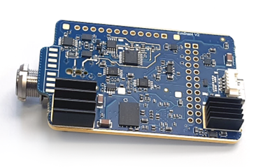
Heat Dissipation
The EmStat4 HR requires two heatsinks to be present on the golden pads at the bottom of the PCB.
The board comes standard with the following two heatsinks from Fischer Elektronik: part numbers ICK PLCC 28 and ICK SMD F 10 SA.
| It is recommended to ensure a steady airflow over the heatsinks when running measurements for a long duration (>10 minutes) with the 100 mA range enabled. |
Links
Design resources
The 3D model and Altium symbol and PCB footprint can be found in the download section of our website: https://www.palmsens.com/emstat4m
Accessories
SPE-connector: DS1020-03ST1D