EmStat Pico Specifications
This page will detail the technical specifications of the EmStat Pico module. This page is based on the datasheet provided on the EmStat Pico product page.
Features
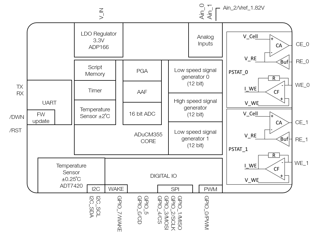
Analog
-
5 analog inputs including 2 high impedance (1 TΩ)
-
2 current measurement channels each with max. current of ±3 mA and min. resolution of 5.5 pA on lowest current range
-
16-bit, analog-to-digital converter (ADC)
-
Two 12-bit voltage output DACs, range 0.2 to 2.4 V (±2.2 V voltage potential to sensor)
-
Two potentiostat circuits with impedance measurement capability <10 Ω to 100 MΩ,
-
0.016 Hz to 200 kHz
-
Internal temperature sensor, ±2°C accurate
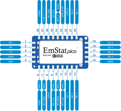
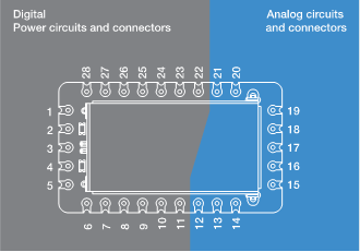
Pin functions
| Pin No. |
Name | Type | Description |
|---|---|---|---|
1 |
N/C |
Reserved |
Factory use only |
2 |
RX |
DIO |
UART receive. Baud rate: 230400 Bd |
3 |
TX |
DIO |
UART transmit. Baud rate: 230400 Bd |
4 |
/DWN |
DIO |
Initiates bootmode. Firmware download begins on exiting reset. (Active Low). This pin is pulled up to 3.3 V by a 10 kΩ resistor. |
5 |
/RST |
DIO |
Resets the module processor. (Active Low). This pin is pulled up to 3.3 V by a 10 kΩ resistor. |
6 |
GPIO_0 |
DIO |
General-Purpose Input/Output Port 0 / PWM Output. This pin defaults as tri-state. |
7 |
GPIO_1 |
DIO |
General-Purpose Input/Output Port 1 / SPI_MISO. This pin defaults as tri-state. |
8 |
DGND |
GND |
High speed digital signal GND return. The module has a single continuous Gnd plane. |
9 |
GPIO_2 |
DIO |
General-Purpose Input/Output Port 2 / SPI_CLK. This pin defaults as tri-state. |
10 |
GPIO_3 |
DIO |
General-Purpose Input/Output Port 3 / SPI_MOSI. This pin defaults as tri-state. |
11 |
GPIO_4 |
DIO |
General-Purpose Input/Output Port 4 / SPI_CS. This pin defaults as tri-state. |
12 |
CE_1 |
V_out |
Potentiostat 1 output. This pin is connected to a Counter Electrode when measuring electrochemical sensors. Optionally, this pin can be used as a DAC output. |
13 |
WE_1 |
I_in |
Potentiostat 1 current measurement TIA input. For electrochemical measurements this pin is connected to the Working Electrode. |
14 |
RE_1 |
V_in |
Potentiostat 1 high impedance reference input. For electrochemical measurements this pin is connected to the Reference Electrode. Optionally, this pin can be used as an ADC input. If unused, it is recommended to connect this pin to AGND. |
15 |
AGND |
GND |
Analog signal Gnd. The module has a single continuous Gnd plane. |
16 |
RE_0 |
V_in |
Potentiostat 0 high impedance reference input. For electrochemical measurements this pin is connected to the Reference Electrode. Optionally, this pin can be used as an ADC input. it is recommended to connect this pin to AGND. |
17 |
WE_0 |
I_in |
Potentiostat 0 current measurement TIA input. For electrochemical measurements this pin is connected to the Working Electrode. |
18 |
CE_0 |
V_out |
Potentiostat 0 output. This pin is connected to a Counter Electrode when measuring electrochemical sensors. Optionally, this pin can be used as a DAC output. |
19 |
Ain_2 |
V_in |
ADC Input / 1.82 V buffered voltage reference. Decouple reference to GND via a 100 pF capacitor. The maximum load current = 200 μA. |
20 |
Ain_1 |
V_in |
ADC Input. |
21 |
Ain_0 |
V_in |
ADC Input. |
22 |
GPIO_5 |
DIO |
General-Purpose Input/Output Port 5. This pin defaults as tri-state. |
23 |
GPIO_6/CD |
DIO |
General-Purpose Input/Output Port 6. Card Detect input for use with SD cards. This pin defaults as tri-state. |
24 |
GPIO_7 |
DIO |
General-Purpose Input/Output Port 7 / WAKE. This pin is pulled up to 3.3 V in Sleep and Hibernate modes and is used to wake the device. This pin defaults as tri-state. |
25 |
I2C_SCL |
DIO |
Interface Clock for I2C. This pin is pulled up to 3.3 V by a 10 kΩ resistor. |
26 |
I2C_SDA |
DIO |
Interface Data for I2C. This pin is pulled up to 3.3 V by a 10 kΩ resistor. |
27 |
V_IN |
Power |
3.5 V to 5.5 V vs GND. |
28 |
DGND |
GND |
Power supply GND return. Module has a single continuous GND plane. |
Absolute maximum ratings
| Parameter | Rating |
|---|---|
V_IN to GND |
-0.3 V to +6.5 V (see ADP166) |
Analog Input Voltage to GND |
-0.3 V to +3.6 V |
Digital Input Voltage to GND |
-0.3 V to +3.6 V |
Total Positive GPIO Pins Current |
30 mA |
Total Negative GPIO Pins Current |
-30 mA |
Storage temperature |
-65 °C to +100 °C |
Operating temperature |
-40 °C to +85 °C |
ESD Human Body Model (HBM) |
4 kV |
ESD Field-Induced Charged Device Model (FICDM) |
1 kV |
Hand Soldering (10 seconds per pin) |
400 °C |
Reflow temperature |
245 °C |
Stresses at or above those listed under Absolute Maximum Ratings may cause permanent damage to the product. This is a stress rating only; functional operation of the product at these or any other conditions above those indicated in the operational section of this specification is not implied. Operation beyond the maximum operating conditions for extended periods may affect product reliability.
Electrical specifications
| Parameter | Min | Typ | Max | Unit | Details |
|---|---|---|---|---|---|
ADC |
|||||
Input Voltage Range |
0.2 |
2.1 |
V |
||
Data Rate |
800 |
kSPS |
|||
Resolution |
16 |
Bits |
|||
Analog inputs |
|||||
Leakage Current |
-1.5 |
±0.5 |
1.5 |
nA |
Ain_0 to Ain_3, WE_0, WE_1 (OFF) |
Leakage Current |
±10 |
pA |
RE_0, RE_1 |
||
EIS measurement |
|||||
Frequency range |
0.016 |
200k |
Hz |
||
Excitation Amplifier Bandwidth |
3 |
MHz |
|||
Impedance Measurement Range |
10 |
10M |
Ω |
||
Potentiostat circuit |
|||||
WE Input Bias Current |
80 |
300 |
pA |
WE input, 25 °C |
|
RE Input Bias Current |
10 |
pA |
RE input, 25 °C |
||
Offset voltage |
50 |
150 |
μV |
||
Source/Sink current |
-3 |
3 |
mA |
||
Applied potential accuracy |
0.04 |
0.2 |
% |
||
Current Range accuracy |
0.1 |
< 0.5% |
% |
±0.1% of range offset |
|
Max bandwidth > 100 nA CR |
100 Hz |
||||
Max bandwidth 100 nA CR |
16 Hz |
||||
Potentiostat circuit |
|||||
WE Input Bias Current |
1 |
nA |
WE input, 25 °C |
||
RE Input Bias Current |
10 |
pA |
RE input, 25 °C |
||
Offset voltage |
50 |
150 |
μV |
||
Source/Sink current |
-3 |
3 |
mA |
||
Applied potential accuracy |
0.1 |
0.5 |
% |
||
Current Range accuracy |
0.2 |
1.0 |
% |
±0.1% of range offset |
|
Max bandwidth > 6 μA CR |
10 |
3000 |
kHz |
||
Max bandwidth 6 μA CR |
5 |
kHz |
|||
Max bandwidth 1 μA CR |
800 |
Hz |
|||
Max bandwidth 100 nA CR |
80 |
Hz |
|||
DAC |
|||||
Resolution |
12 |
Bits |
|||
Voltage Range (Low speed) |
0.2 |
2.4 |
V |
||
Voltage Range (High speed) |
±0.607 |
V |
On a bias point fixed by the Low Speed DAC |
||
Low and High Combined |
0.2 |
2.8 |
V |
||
Buffered reference voltage output |
|||||
Voltage |
1.815 |
1.82 |
1.825 |
V |
TA = 25°C, capacitive load to ground 100 pF |
Load Current |
200 |
μA |
|||
GPIO |
|||||
Input Voltage Low |
0.825 |
V |
|||
Input Voltage High |
1.88 |
V |
|||
Output Voltage Low |
0.3 |
V |
Sink current = 2 mA |
||
Output Voltage High |
2.9 |
V |
Source current = 2 mA |
||
Short-Circuit Current |
11.5 |
mA |
|||
Temperature sensor (default ADuCM355) |
|||||
Resolution |
0.3 |
°C |
|||
Accuracy |
±2 |
°C |
|||
Temperature sensor (optional ADT7420) |
|||||
Resolution |
0.0078 |
°C |
|||
Accuracy |
±0.25 |
°C |
|||
Power requirements |
|||||
V_IN voltage range |
3.5 |
5 |
5.5 |
V |
|
Normal (High speed 1 Chan) |
30 |
mA |
|||
Normal (Low speed 1 Chan) |
10 |
mA |
|||
Normal (Low speed 2 Chan) |
15 |
mA |
|||
Sleep (Static 1 Chan) |
8 |
mA |
|||
Sleep (Static 2 Chan) |
13 |
mA |
|||
Hibernate mode |
10 |
μA |
For more detailed specs see datasheets for ADuCM355, ADT7420, ADP166 and AD8606.
Power supply
The EmStat Pico has an on-board 3.3 V LDO (ADP166) and supply filtering. This provides clean operation from a USB or a 3.5 V to 5.5 V supply. Driving the EmStat Pico V_IN directly from a switching regulator may introduce measurement noise. Care should be taken to provide clean power to the V_IN pin.
| Power modes | |
|---|---|
Normal mode |
CPU running. PSTAT channels configured by the user (OFF, OCP, Low Speed, High Speed). Measurement performed. |
Sleep mode |
CPU is not running. PSTAT channels configured by the user (OFF, OCP, Low Speed, High Speed). All voltages are still applied, but no measurements can be done. |
Hibernate |
CPU is not running. PSTAT channels are OFF. |
Digital interface
The EmStat Pico features the following digital interfaces:
-
UART with baud rate of 230400 Bd
-
SPI port with SD card support. (EmStat Pico as master only). For SPI timings see ADuCM355.
-
I2C port. (EmStat Pico as master only). Note: The ADT7420 temperature sensor is connected to this bus and both the SCL and SDA lines have 10 kΩ pullup resistors to 3.3 V
-
1 PWM output
-
8 GPIO
Calibration
The EmStat Pico has on-board 1 kΩ and 100 kΩ precision resistors (accuracy: ±0.1%, temperature coefficient: ±25 ppm/°C) for self-calibration.
Analog interface
DAC modes
The EmStat Pico has 2 low speed DACs and one high speed DAC. The 2 low speed DACs have an output range of 0.2 V to 2.4 V and can be used simultaneously. The single high speed DAC has an output range of ±0.607 V on a bias point fixed by the low speed DAC.
A low speed DACs and the high speed DAC can be combined to achieve an output range 0.2 V to 2.8 V. This can be done on one channel at a time.
Potentiostat channels
The applied cell potential is the voltage between RE and WE (voltage supplied at CE and controlled at RE by potentiostat loop) of the Potentiostat Channel. WE is maintained at a potential between 0.819 V and 2.366 V to allow headroom for the TIA to operate. Thus the applied potential ranges are:
high speed DAC: -1.981 V to 2.166 V.
low speed DAC: -1.581 V to 2.166 V.
The EmStat Pico uses the 2 potentiostat channels of the ADuCM355 with the addition of high impedance buffers (AD8606) on the RE inputs. See links below for further details.
Analog inputs
The EmStat Pico features a 16-bit, 800 kSPS, successive approximation register (SAR) analog-to-digital converter (ADC) with multiplexer, input buffers, built-in anti-aliasing filter (AAF), and programmable gain amplifier (PGA). The input range of 0.2 V to 2.1 V. The multiplexer switches between the analog input channels (Ain_0 to Ain_2) and the current and voltage measurement channels of PSTAT_0 and PSTAT_1. For further details see ADuCM355 documentation.
Layout
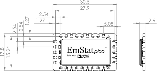
Surface mount PCB footprint
Figure 6 shows the recommended SMT footprint for the EmStat Pico for hand soldering directly to a PCB using the castellated pads. Pads are 3 mm long by 1.5 mm wide.

Through hole PCB footprint
Figure 7 shows the recommended through hole footprint for the EmStat Pico for mounting with Samtec TS-112-T-A-1 pins. Pads are 1.5 mm diameter with 0.8 mm diameter hole spaced on a 2.54 mm (100 mil) grid.
Layout considerations
The EmStat Pico has 3 GND pins. Pin 28 is the power supply GND return. Pin 8 is located beside the SPI lines to provide a high speed digital GND return. Pin 15 is located beside the Analog pins to reference single ended analog signals and to connect to external shielding. The module has a single continuous GND plane, so all 3 pins are connected together.
When laying out a PCB to carry the EmStat Pico it is recommended to use a single continuous GND plane and to zone the board as shown in Figure 8. If desired, separate analog and digital GND planes can be used with the EmStat Pico providing the connection between the two planes.
Assembly
SMT board-to-board soldering
The EmStat Pico has castellated pads on each side to allow surface mount board-to-board soldering. It is recommended to use hand soldering onto the footprint detailed above using a 1.2 mm chisel tip at 370°C and dwell for no more than 10 seconds on each pad.
SMT reflow information
The EmStat Pico has a Moisture Sensitivity Level (MSL) of 3.
Recommended reflow temperature is maximum 245 °C.
Pin mount
The EmStat Pico through hole pads have an internal diameter of 0.76 mm (30 mil). These are designed to accept 0.64 mm (25 mil) diameter pins such as Samtec TS-112-T-A-1. The through hole pads are located on a 2.54 mm (100 mil) grid to match standard prototyping board. It is recommended to hand solder the pins into the EmStat Pico using a 1.2 mm chisel tip at 370°C and dwell for no more than 10 seconds on each pad. Use Low Residue Tin (No-Clean Flux Core Solder).
Links
Module components
TS-112-T-A-1:
https://www.samtec.com/products/ts-112-t-a-1
Design resources
The 3D model and Altium symbol and PCB footprint can be found in the download section of our website: https://www.palmsens.com/pico
Accessories
-
USB to UART convertor:
UMFT234XD-NC -
SPE connector:
DS1020-03ST1D
See for more accessories: